
GINTI launches fully fledged 3D stacking LSI fabrication service
The Global Integration Initiative (GINTI), a center equipped with facilities and an environment for R&D, prototyping and pilot production of 3D stacked LSIs, started a full-service operation in Miyagi Prefecture in April.
Tohoku University established GINTI at Miyagi Fukko Park*, Tagajo, Miyagi Prefecture, at a cost of several billion yen, including a subsidy of 1 billion yen (US$10 million**) from the Ministry of Economy, Trade and Industry (METI). The center opened last September.
*A research park established as a recovery initiative in the aftermath of the Great East Japan Earthquake of 2011.
**Original figures are in Japanese yen. The exchange rate is roughly US$1=100 yen.
"We've been providing 3D IC prototype fabrication services to a few customers. Now we're ready to offer fully fledged services. We've already received almost 40 orders for prototype manufacturing from customers in Japan and overseas," said Professor Mitsumasa Koyanagi of Tohoku University's New Industry Creation Hatchery Center who is the director of GINTI.
GINTI has all the necessary equipment for 3D LSI fabrication, ranging from TSV fab process and bonding and assembly process to test process. These facilities offer customers the flexibility to fabricate 3D stacked LSI prototypes from chip-level to 200/300mm wafer-level to meet their particular requirements.
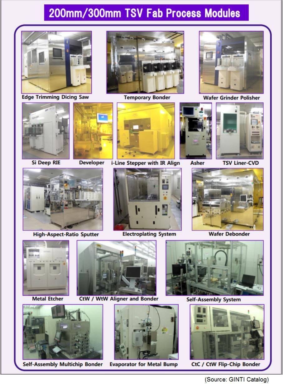
GINTI already has a self-assembly system for 200mm wafers. "We are now developing a self-assembly system for 300mm wafers, which we will complete by the end of this fiscal year," said Koyanagi.
GINTI's current capacity is about 1,000 wafers per year (in 300mm wafers). But the 1500m2 cleanroom can accommodate greater capacity. GINTI intends to expand annual capacity to 3,000 wafers within a few years. It envisages eventually installing multiple units of all process equipment to raise capacity to 10,000 wafers per year.
"I believe GINTI is unique in the world in its ability to offer comprehensive processes for 3D LSI prototype fabrication. We've received another 25 inquiries for prototyping. The rise of 3D stacked LSIs should result in a rising tide of orders for our services. To cope with the anticipated growth in demand, we will recruit more people to run the prototyping support service system," said Koyanagi.
3D stacking of heterogeneous chips
The 3D stacked structure is already used for some NAND and DRAM memories, but 3D stacking of logic and analog LSIs still faces several challenges. The defect recovery technology employed for memories is not applicable to 3D stacked LSIs. Chip sizes differ, making it difficult to stack non-memory ICs at a high yield rate with high reliability and at low cost.
Koyonagi's research team proposes a self-assembly 3D stacking method to stack known good die (KGD) chips on a wafer. Taking advantage of the surface tension of liquid droplets, multiple KGD chips are aligned and set on a substrate wafer in a batch. The method aligns KGD chips of different sizes and different types, such as MEMS and sensors, for stacking.
GINTI's self-assembly system can stack more than 500 chips on a 200mm wafer in a batch within one second with alignment accuracy of 0.5-1 micron. GINTI intends to refine the accuracy to 0.1 micron and develop equipment for 300mm wafers with a view to applying the technology to volume production lines.
Related sites:
Global Integration Initiative (GINTI)
GINTI Catalog
Three-Dimensionally Stacked Hetero-Chip Fabrication by Self-Assembly
The original article in Japanese appeared in the June 18 issue of The Semiconductor Industry News. Edited and translated by EmergingTech, which added the figure, linkes and notes.
Warning: Invalid argument supplied for foreach() in /home2/semicon/hosting/spiwww/include/Banner.php on line 78
Warning: array_multisort(): Argument #1 is expected to be an array or a sort flag in /home2/semicon/hosting/spiwww/include/Banner.php on line 81
Warning: Invalid argument supplied for foreach() in /home2/semicon/hosting/spiwww/include/Banner.php on line 85