KEYNOTE/INVITED SPEECH
ISSM 2010 featured keynote speakers that spanned a broad spectrum of industry leadership and technology innovation.
"3D-TSV Overview"
Dr. Sitaram Arkalgud
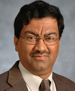
Director, 3D Interconnect, SEMATECH
Abstract
Biography
Dr. Sitaram Arkalgud has served as Director, 3D Interconnect of SEMATECH since 2007. While on assignment to SEMATECH from Qimonda/Infineon Technologies, Arkalgud directed SEMATECH’s Interconnect division for three years, during which time he led efforts to screen, characterize, and improve the performance of low-k dielectric materials for the ITRS 45 and 32nm technology generations, and also initiated the exploration of next-generation 3D interconnects.
Prior to his assignment at SEMATECH, Arkalgud served as Infineon’s director of the MRAM Development Alliance between Infineon and IBM. Earlier, he worked as a Technology Officer for the Memory Products Division and product manager for Ferroelectric RAM development at Infineon. Arkalgud came to Infineon from Motorola Inc., after working for nine years in several advanced logic and memory projects.
The author of more than 26 publications and presentations, and holder of 14 U.S. patents, Arkalgud earned a doctorate and master’s degree in materials engineering from Rensselaer Polytechnic Institute in Troy, NY, and a bachelor’s degree in metallurgical engineering from Karnataka Regional Engineering College, Suratkal, India.
"Relentless Innovation: The Case for Agility in Semiconductor Manufacturing"
Thomas Sonderman

Vice President, Manufacturing Systems and Technology,
GlobalFoundries
Abstract
As the market for advanced technology continues its endless march forward, the industry faces increasing challenges to sustain the current pace of innovation. Leading-edge process technology is becoming more cost-intensive, design companies are developing chips with extraordinary complexity, and the next generation technology will require an unprecedented level of performance, and cost-effectiveness to deliver on its full potential. This confluence of factors is compounded by a major global recession, which has caused many manufacturers to develop a renewed focus on short-term productivity improvements. However, there is still a critical need for manufacturers to become more agile so that they are better positioned to respond to the long-term challenges of fluctuating demands. To address this need for agility, GLOBALFOUNDRIES has developed a unique manufacturing capability, called "Automated Precision Manufacturing", or APM. Through enhanced delivery capabilities and improved product quality, APM has enabled GLOBALFOUNDRIES to deliver cutting-edge technology at low costs, which is a critical manufacturing advantage in the fast moving semiconductor industry. This presentation will take a look at how the lean manufacturing techniques that have successfully been used to transform other industries can be leveraged to provide the agility needed in semiconductor manufacturing.
Biography
Thomas Sonderman is Vice President of Manufacturing Systems and Technology at GLOBALFOUNDRIES. In this role, he has global responsibility for development, integration, support and scalability of the company’s 300mm Automated Precision Manufacturing (APM) technologies and associated systems, focusing on maximizing operational efficiencies without sacrificing velocity.
Sonderman joined GLOBALFOUNDRIES after more than 15 years with AMD, where he held numerous management and engineering positions. Most recently he served as Director of APM Technology.
Prior to joining AMD, Sonderman worked as a process control engineer for Monsanto Chemical Inc. He has a broad range of experience in the area of manufacturing automation and its application to high-volume semiconductor fabrication. He is a highly sought-after speaker at industry conferences and is a member of two advisory committees at the University of Texas: Chemical Engineering & Science and Technology & Society. Sonderman is the author of over 45 patents and has published numerous articles in the area of automated control and manufacturing technology.
Sonderman received a bachelor’s in chemical engineering from the Missouri University of Science and Technology in 1986 and a master’s in electrical engineering from National Technological University in 1991.
"Technologies and trends related to Power Module"
Dr. Katsumi Sato
Senior manager, Power Device Development Department,
Power Device Works Mitsubishi Electric Corp.
Abstract
A demand to realize low carbon society becomes very strong. For CO2 reduction, energy saving and/or the new energy product used new technology such as Photovoltaic power generation technology and wind power generation technology have been introduced to the market. The power electronics is main technology for the energy-saving and will progress more in future. The power device with high power capability such as IGBT is a key component in power electronics technology and will progress more with progress of the application field. I introduce a trend of the IGBT and both wafer process technology and package technology to support high performance IGBT.
Biography
Katsumi Satoh joined Mitsubishi electric corp. in 1984. He previously worked on development of high power semiconductor such as a high voltage thyristor, a light triggered thyristor, GTO and GCT for high power transmission system in Mitsubishi Electric Corporation. His current research interests include power device chips technology and packaging technology for power modules. He received Doctor of Engineering degree from Kyusyu University, Japan in 2000. He received First Prize Paper Award from IEEE in 2001.
"Smartgrid for future green society"
Takeshi Yokota
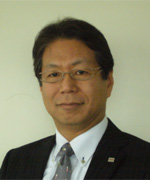
Technology Executive, T&D Power Systems,
Transmission Distribution & Industrial Systems Company
Toshiba Corporation
Abstract
To reduce the CO2 emission, to save the energy, and to reduce fossil fuel usage are critical requirements for future green society. Smartgrid is one of technology to realize these matters. Semiconductor technology is also very important measures to contribute these Smartgrid products. Prospects of Smartgrid and the impacts to semiconductor business will be presented as a keynote speech.
Biography
Takeshi Yokota works as a technology executive of Transmission, Distribution and Industrial System Company of Toshiba Corporation. He received his BS degree and MS degree of electrical engineering from Yokohama National University in 1980 and 1982 respectively. He joined Toshiba Corporation in 1982, and has been engaging in substation engineering work and the development of substation equipment such as SF6 gas-insulated transformer and gas-insulated switchgear and recently focused on global T&D business and Smartgrid business. Since 2007, he has been working as a convener of CIGRE B3.22 WG (UHV substation). He is a member of IEE of Japan, CIGRE, IEC, and IEEE.
"Advanced Process Control for Nano Technology Manufacturing"
Dr. John Kibarian
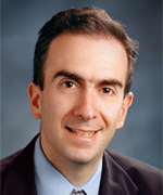
President and CEO PDF Solutions
Abstract
The electronics industry has been on a transition path to nano scale manufacturing to improve device performance, operation efficiency and reduce manufacturing cost. Mega scale semiconductor, LED, LCD and PV fabs all share the similar requirement to achieve the highest degree of process control.Currently, inline metrology and tool FDC data are the main information source which engineers use to conduct the process control. However, metrology data are very expensive in terms of their tool cost and its hit on cycle time. Moreover, metrology measurement accuracy is increasingly questionable due to the rapid device shrinking factor. All leading fabs are employing EES/FDC system to provide real time information of the wafer status for feedback, control and process optimization. However, they are expensive to setup and maintain due to its high IT infrastructure and human monitoring cost. They are also prone to frequent missing and false alarms.
In this discussion, we will address potential solutions for more effective process control in the maga fabs. We believe, a new generation of advance process control system is required for all new generation fabs:
- We will need a more effective fab wide EES/FDC network. Rather than monitor process on a single tool and recipe base, we need to monitor the whole process flow on a holistic base and achieve product performance/yield relevant process control. This methodology will require centrally controlled tool data collection, analysis and monitor. EES/YMS data integration and correlation will enable performance/yield focused tool control by dynamically control the key process in the whole process.
- Given the shrinking process margin in nano manufacturing, we will require more items to be monitored on a regular basis. Our expectation is a combination of in-line and EOL characterization and model-based process control & diagnostics. Inline virtual metrology based on physical model is required to greatly enhance the metrology practice and provide data source for dynamic process control like R2R.
The electronics industry is becoming one of the most capital-intensive industries. A well designed fab-wide control framework provides improved competitiveness of the manufacturers as they transition to nano scale manufacturing. This transition provides exciting challenges and opportunities to engineers to develop a new process control paradigm for the industry.
Biography
John K. Kibarian, Ph.D., one of our founders, has served as President since November 1991 and has served as our Chief Executive Officer since July 2000. Dr. Kibarian has served as a director since December 1992.
Dr. Kibarian received a B.S. in Electrical Engineering, an M.S. E.C.E. and a Ph.D. E.C.E. from Carnegie Mellon University.
"More-than-Moore reinvented"
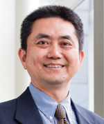
George Liu
Director of Power/ MEMS Business Development Division
Taiwan Semiconductor Manufacturing Corporation (tsmc)
Abstract
MtM is an old field, but it has a new life now. Green requirement, cloud computing, and natural world interfaces demand for much more sophisticated MtM solutions. This trend presents both challenges and opportunities for IDM’s, fabless companies, and foundries.
To meet these new expectations for MtM, we need high tech solutions which include advanced process modules, comprehensive design kits, precise manufacturing control, and timely customization service.
To compete effectively in the future MtM field, large scale manufacturing, smaller device foot print, and feature rich integration become more important. Foundries capable of delivering competitive solutions will offer a level playing field to both IDM’s and fabless companies.
TSMC is committed to provide competitive MtM solutions to IDM’s and fabless companies, for diversified applications, and for the long term.
Biography
Mr. George Liu joined TSMC in February 2007 as the Director of Mainstream Technology Business Development. Since then, he has taken charge of More-than-Moore technology, which includes MEMS, Power IC, eFlash, and display drivers.
George brings 25 years of experience in the IC industry to TSMC. He started at Intel in 1983, where he spent 19 years managing various projects in design, fab, assembly, and procurement. Among these projects were 8/16bit MCU design, multi-processor chipset architecture, and a China factory startup.
In 2002, he took an entrepreneurial opportunity and joined Primarion, a power IC startup company, as Vice President of Operations and Asia Sales. In 2 years, he established digital control acceptance and a solid customer base.
Prior to joining TSMC, George worked for 3 years as Vice President of Corporate Development at Vanguard International Semiconductor, a TSMC subsidiary company. During this period, he built a design service team, an enhanced IT infrastructure, and a few strategic alliances.
Mr. Liu holds a B.S. in physics from National Taiwan University, and an MSEE from Arizona State University.
"Perspective of CMOS Technology"
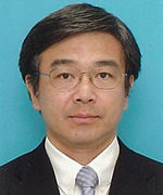
Tohru Mogami
General Manager,
Semiconductor LeadingEdge Technology (Selete), Inc.
Abstract
In Si-LSI industry, the variation of device characteristics has been one of the issues, and it has been continuously developing the several methods to mitigate and straighten out it. Currently, the local and random variation has been still the critical issue, compared to the global variation and the systematic one. The main mechanisms in that variation can be line edge roughness (LER) and random dopant fluctuation (RDF). Both LER and RDF are related to a lot of process technologies. In order to analyze the relationship between this variation and process technology and to reduce the variation, we should develop the new analysis methods for variations in <50nm CMOS devices and the new control methods. I will present the current status of variations and variation mechanisms, and discusses future requirements for the advanced CMOS-LSI.
Biography
Tohru Mogami joined Microelectronics Research Laboratories, NEC Corporation in 1982, where he has been engaged in research and development of VLSI processing and device technologies. He developed and presented many advanced technologies for the advanced-generation Si-CMOS. In 2006, he moved to Selete Incorporation. He has managed the advanced LSI device programs, including the variation control technologies of transistors, the development of CNT interconnects and optical interconnects. He has contributed to "Symposium on VLSI Technology", which is one of the premium conferences in Semiconductor field, and played as Program chair in 2007 and Symposium Chair in 2009 in Kyoto. He received Fellow Award of JSAP in 2010.
Mr. Liu holds a B.S. in physics from National Taiwan University, and an MSEE from Arizona State University.


