KEYNOTE SPEAKER
Monday, October 15
What did I explore in Half a Century of Research?
Dr. Leo Esaki
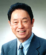
Nobel Laureate in Physics
President, Yokohama College of Pharmacy
Chairman, The Science and Technology Promotion Foundation of Ibaraki
Abstract
In 1947, after graduation in Physics, the University of Tokyo, I explored the possibility of putting quantum principles into practice in the electronics industry, which was a rather unique venture at that time. At Totsuko (presently SONY), Tokyo, in the course of tunneling study in narrowing the p-n junction width down to 10 nanometers, the Esaki tunnel diode - the very first quantum electron device - came as a total surprise in 1957. In recognition of this discovery the 1973 Nobel Prize in Physics was awarded.At IBM Watson Research Center, New York, we pioneered research on superlattices and quantum wells in the 1970s and the early 1980s, setting off a wide variety of experimental and theoretical investigations worldwide, resulted in not only the observation of a number of intriguing new phenomena such as Bloch oscillation due to electric quantization, but also the emergence of a new class of transport and optoelectronic devices such as high electron-mobility transistors (HEMT), high-speed resonant tunnel diodes, high-performance injection lasers with quantum wells, and quantum cascade lasers. In recognition of this invention, the APS 1985 Int. Prize for New Materials, the 1991 IEEE Medal of Honor and the 1998 Japan Prize were awarded.
Since the superlattice periods or the quantum well-widths are on the nanometer scale, the studies have served as the precursor to a variety of nanostructures.
Toshiba's Semiconductor and Storage Products Strategy and the Renovation of the Semiconductor Industry in Japan.
Shozo Saito
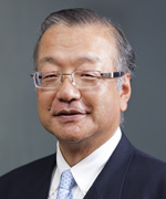
Director, Representative Executive Officer, Corporate Senior Executive Vice President, Toshiba Corp.
Abstract
In the coming age of the Smart Community Society, we will have to make practical use of Big Data. Toshiba is the only company with capabilities in both semiconductors and storage products, a strong point that gives us advantages in developing and executing strategies for total innovation in storage.
In recent years, Japanese companies have lost share in the world semiconductor market, as U.S. and Asian companies have increased theirs. We propose a business model of the sort required to revitalize Japan's semiconductor industry.
The 20th Anniversary Speech
ISSM - Accelerator from "Know-how" to "Science"
Yasuo Mizokami
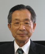
Representatives, Molecular Imprints Japan
Tuesday, October 16
Technologies and Business Strategies of IT Industry in the Future
Yoon Woo Lee
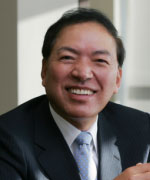
Executive Advisor, Samsung Electronics Co., Ltd.
Leading through the present, anticipating the future
Shizuo Igarashi
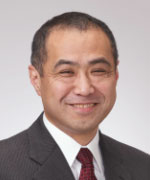
General Manager, Manufacturing and Technology, Texas Instruments Japan Ltd.
Abstract
From the decision to extend its manufacturing footprint with strategic foundry relationships to opening the industry's first dedicated 300mm analog wafer fab, TI has managed to lead through the dynamic and ever-evolving semiconductor market. Even through times of great chaos and uncertainty, such as the financial uncertainty in 2008/2009 and the devastating 2011 earthquake and tsunami in Japan, TI's ability to anticipate change and lead through crisis gives customers the assurance that TI will support them today and well into the future. TI's leadership in embedded processing and analog semiconductors is the result of the company's clear strategy and focus on providing customers the broadest, deepest semiconductor portfolio of innovative products, strong customer support through a global sales force and a manufacturing model that ensures continuity of supply in any market environment. Today, TI is well positioned to help its 80,000 customers unlock the possibilities of the world as it could be - smarter, safer, greener, healthier and more fun.
Evolution of Semiconductor Device Technologies and the Revolution needed in Manufacturing
Raj Jammy
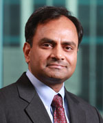
Vice President of Materials and Emerging Technologies, SEMATECH
Wednesday, October 17th
Innovations on Advanced Sub-system Integration
Douglas Chen-Hua Yu, Ph.D.
Senior Director, Integrated Interconnect and Package Division, R&D, Taiwan Semiconductor Manufacturing Co., Ltd.
European Vision and Achievements Towards Larger Diameter Wafers
Prof. Dr.. Lothar Pfitzner

Head of "Semiconductor Manufacturing Equipment and Manufacturing Methods" at Fraunhofer Institute of Integrated Systems and Device Technology, Erlangen, Germany


