Keynote Speech
December 2nd
"TSMC perspective on 3D packaging trend and solutions"
Dr. Cliff Hou

Vice President, Research & Development / Design and Technology Platform, TSMC
Abstract
As the trajectory of Moore's Law marches toward single-digit nanometer era, the tried-and-true two-dimensional scaling is encountering challenges that necessitated integration schemes along the third dimension.
In this talk, we will offer a foundry's perspectives on 3D IC. From the historical trend of system miniaturization and scaling, we see the need for combined design and packaging solutions for both high-performance and mobile / low-power applications. We then introduce TSMC offering: CoWoS and InFO tailored for high performance and mobile applications, respectively. Each technology is then described in more details to give the audience a closer look at the construction, advantages, flexibility, applications and design solution. We conclude the talk with the technology readiness as well as a glimpse into the future.
"Application of power semiconductors to railway field as a forerunner of finding answers of emerging issues"
Prof. Tomoki Watanabe
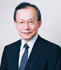
Professor
Endowed Chair by JR-East
Department of Electrical and Electronic Engineering, Graduate School of Science and Engineering, Tokyo Institute of Technology
Abstract
Electric railway development has been synchronized with the development of electrical engineering. Nowadays power converters with SiC semiconductor device have been already put into the railway market.
The size of railway industry market is around two hundred billion dollars and its steady growth is prospected. High performance converters are needed for high-speed railway but the market is limited. For main line and urban railway the market is huge, but the lowest price is required to get the contract.
Railway is an infrastructure business. Outside of Japan, there are involvements of the governments for the railway related contracts in general, and piles of standards are cited for the specifications. In Japan, majority of railway companies are private ones and there is a tendency that the railway companies decide the specifications by their own way. These have a significant influence on the railway industry business.
In the semiconductor manufacturing industry there are not only semiconductor manufacturers but also material suppliers and semiconductor facility suppliers. Additionally there is a trend of production specialization among semiconductor manufacturers. In parallel with the standardization of semiconductors and semiconductor manufacturing processes, the semiconductor facility suppliers have taken a larger role.
For the semiconductor manufacturers to step up its presence in the market, it is important to have the appealing competitiveness of prices, functions or brands.
Added values of semiconductors are buried in a heap of needs of final users. Onboard power converters consist of power parts like power semiconductors and control parts, and either malfunction stops the power converters, which result in a significant loss of railway operation. There are strong and persistent needs for the zero faults during maintenance interval and the maintenance cost reduction. An appropriate fault/age prognostic can be a promising added value. Another candidate of added value is an electromagnetic noise free solution. Emissions of existing power converters are not compatible with other electronic devices in general. Innovations in this field with circuit topologies are awaited.
High-value added products are welcomed first in Japanese market like mobile phones.
Manufactures can utilize Japanese market as an incubator and the big challenge is how to combine this with the world huge market.
"Hitachi's Social Innovation Business"
Akihiko Tobe
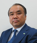
General Manager, Social Innovation Business Project Division, Hitachi, Ltd.
Abstract
Since its early beginnings over 100 years ago, Hitachi's corporate credo has been "contributing to society through the development of superior, original technology and products." Over the years, that mission has led Hitachi to develop a host of products, services and solutions that address a wide range of infrastructure challenges. Society's need for advanced technologies is constantly evolving; in turn, so is Hitachi. With its determination to improve the quality of life for the global community, Hitachi decided to focus on the Social Innovation Business.
Through the Social Innovation Business, Hitachi hopes to provide total solutions for sustainable, urban development worldwide and to address critical global issues such as the need for creating and improving the transportation infrastructure in urban areas, improving access to clean water, developing technologies that promote a smooth and efficient transition to the Smart Grid while keeping a sharp eye on sustainability objectives and the conservation of our world's supply of precious natural resources.
Hitachi will collect a variety of data in the city through the sensing of technology, will introduce through the case of town planning the development of technology by leveraging the big data. That the needs of the intelligence of the sensor is increasing will also affect the semiconductor.
December 3rd
"200mm Opportunities and Challenges in New Era"
Leuh Fang

President, Vanguard International Semiconductor Corporation
Abstract
Semiconductor industry has been propelled by various application momentums and Moore's Law plays as an invisible hand for more than 40 years to the industry since it was officially coined in 1970s. High transistors density products like logic and memory comply with Moore's Law well and drive to smaller technology node and larger wafer diameter to get best cost performance ratio. 300mm capacity, in terms of area, with advanced technology nodes by far surplus 200mm 1.8 times and will keep on increasing. However, not all semiconductor segments have to follow the Moore's Law if it cannot create additional value to the segments but accommodate in More than Moore, heterogeneous integration and many complementary approaches well. That leaves plenty of room to legacy technology nodes and 200mm fabs to grow. Especially, the recent hype of the IoT (Internet of Things) and the extral application in the automotive electronics creates a lot of imagination for the demands.
There are opportunities, but also challenges to 200mm Fabs in the new era and they will be addressed in the speech,
- What will the growth momentum generate from 200mm Fabs in the coming years?
- Will those new momentum stay in 200mm and prolong its lifespan?
- Where are the challenges of 200mm?
- If not all 200mm Fabs are created equal then what models may be more sustainable in the new era?
Invited Talk
December 2nd
Highlight Session Keynote : Big Data
"Issues of Big Data in Toshiba S&S Company"
Akio Oka
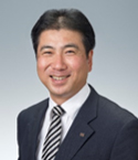
Chief Information Officer, Semiconductor & Storage Products Company, Toshiba Corporation
Abstract
In the Toshiba S&S semiconductor company, in order to maximize an operating revenue and to continuing progress, we are addressing to realize total optimization among the field of research, development, engineering, Monodukuri and sales/marketing.
As a result, when carrying out decision and action in each business processes, practical use of data is performed daily.
The size of data, which is used for the PDCA cycle especially in Monodukuri, is very huge. The Big Data handling technology is indispensable to use this data.
In today's presentation, I would like to intorduce actual examples of the practical utilization of Big Data in Toshiba S&S company, and then to show the issues of Big Data utilization.
December 3rd
Highlight Session : Power Device
"Progress in SiC Power Devices and Manufacturing Technology"
Prof. Tsunenobu Kimoto
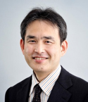
Kyoto University
Abstract
Silicon carbide (SiC) has received increasing attention as a wide bandgap semiconductor for advanced high-power devices. Through recent progress in SiC crystal growth, 100-150 mm wafers with a reduced defect density are commercially available. The device processing such as ion implantation and contacts is reasonably mature since the last decade. High-voltage (600-1700 V) SiC Schottky barrier diodes (SBDs) and power MOSFETs have been released as commercial products, demonstrating remarkable loss reduction in power supplies, photovoltaic converters, industrial motor control, and traction. In R&D, ultrahigh-voltage (> 10 kV) SiC diodes (SBD/PiN) and switching devices (MOSFET/IGBT) have been developed. In crystal growth and device processing of SiC, however, several unique techniques and systems, which are not common in the Si technology, are required. In this paper, the present status and future challenges in SiC power devices and manufacturing technology are presented.
"Intelligent Sampling Decision Scheme Based on the AVM System"
Dr. Fan-Tien Cheng
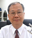
Chair Professor , National Cheng Kung University
Abstract
Reducing sampling rate to as low as possible is a high priority to reduce production cost. Several sampling methods in the literature were proposed to achieve this goal. They utilized real sampling inspections as the representatives for the other related wafers to monitor the whole production process. Under the condition of stable manufacturing process, virtual metrology (VM) may be applied to monitor the quality of wafers while real metrology is unavailable. Therefore, the sampling rate may further be reduced with a sampling decision scheme being designed according to reliable VM. Nevertheless, once a new production variation occurs between planned samplings and no real metrology is available during this period for updating the VM models, un-reliable VM predictions may be produced. The authors have developed the automatic virtual metrology (AVM) system for various VM applications. This paper focuses on applying various indices of the AVM system to develop an Intelligent Sampling Decision (ISD) scheme for reducing sampling rate while VM accuracy is still sustained. Based on the examples of an etching and a PECVD processes in a foundry, the ISD scheme has been proven to be a powerful algorithm that can reduce the sampling rate to one fourth of the original setting and remain comparable VM accuracy simultaneously


