Keynote Speakers
December 12th
"Minimal Fab using half-inch wafers to reduce a fab investment to 1/1,000"
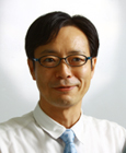
Dr. Shiro Hara

Group Leader, Minimal System Group, Nanoelectronics Research Institute
National Institute of Advanced Industrial Science and Technology (AIST)
Abstract
The minimal fab was designed in order to achieve brand-new semiconductor fab whose investment cost is 1/1,000 of a conventional mega fab. The targets of minimal fab are device markets with high-variation and low-volume. The minimal fab has three important features. (1) The wafer diameter is a half inch. (2) Each process tool size is 294 mm wide x 450 mm deep x 1440 mm high. (3) No clean room is needed due to the use of local clean technology. We have already fabricated CMOS transistors with good electric characteristics using developed minimal tools. This paper describes the concept, development of minimal equipment, the fabrication of devices, and challenges for a practical use as a production line.
CV
Dr. Shiro Hara is the founder of minimal fab concept. In 1993, he became a researcher of Electrotechnical Laboratory, MITI. He developed a local clean research system to find elemental cause of variations of electronic device characteristics. In 2007, he proposed the Minimal Fab concept to reduce an investment cost of a semiconductor factory into 1/1000. He apply the local clean technology to the minimal wafer transfer system. Using this transfer system as the core technology of the minimal fab, he has been developing the minimal fab with around 50 makers. He is the minimal system group leader in AIST, METI. Also, he is the representative of Fab System Research Consortium of AIST. During FY2012-2014, he promoted the national project on the development of minimal system as the project director.
"Toyota's Efforts Toward Realizing a Sustainable Society"
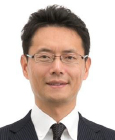
Dr. Takahiro Ito

General Manager, Process Development Dept.,
Power Electronics Development Div.
TOYOTA MOTOR CORPORATION
Abstract
The mass consumption of fossil fuels has followed the progress of global industrial and technological development since the start of the twentieth century.
This has resulted in several issues that we are facing today.
These include environmental issues such as global warming caused by increasing CO2 emissions.
Another issue is the increase in traffic accidents as vehicle ownership grows around the world.
For these reasons, the development of environmental and safety technologies for vehicles is highly important.
Our key advantages consist of the development of next-generation environmentally friendly vehicles using core hybrid technologies, and the promotion of automated driving technology to help realize a society where everyone can move safely, efficiently, and freely.
The power control unit (PCU) and power semiconductors are key technologies for controlling the electrical power of hybrid vehicles.
In particular, we are developing SiC power semiconductors as a promising technology for improving fuel economy and reducing the size of the PCU.
CV
Takahiro Ito received the B.E., M.E. and Ph.D. degrees in electronics engineering from Shizuoka University, Hamamatsu, Japan, in 1994, 1996, and 1999, respectively.
In 1999, He joined Development Dept. No. 42, Electronics Development Div. 4, Toyota Motor Corporation, and was engaged in the development of power semiconductor for hybrid vehicle.
From 2002 to 2004, he was a Researcher of ASET HALCA Project which investigated advanced semiconductor manufacturing called "Mini-Fab".
From 2005 to 2014, he had been involved in the development of Si power semiconductor process. Since 2015, he has been a General Manager of Process Development Dept., Power Electronics Development Div..
And he is currently engaged in research and development of Si and SiC power semiconductor process for next generation vehicle.
"An overview of smart factories in Industry 4.0 implementation."
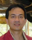
Dr. Jonathan Chang

Senior Director, Backend, Factory Integration, SCM,
Infineon Technologies
Abstract
Manufacturing theory shows that manufacturing performance depends on the capability of deviation control (quantity, speed of detection and speed of recovery). Semiconductor Manufacturing has highest complexity among all manufacturing industries and required highest degree of control competency for all deviation from 4M (man, machine, material and method). It is easy to see the impact of control capability to the manufacturing performance sustainability in term of cycle time, on-time delivery, productivity and quality in semiconductor industry. A smart manufacturing from Industry 4.0 enable advanced control and optimization with high automation and manufacturing science. It shows overall 10%-25% manufacturing cost gap comparing to a factory with mainly human decision, communication and information handling. Industry 4.0 smart manufacturing implementation did not only required effective system development, deployment but also effective manufacturing integration know-how with new effective manufacturing setup and final performance change using new capability.
CV
Jonathan Yung-Cheng Chang has worked in semiconductor manufacturing for more than 20 years, including IT manager and Manufacturing manager in TSMC 200mm FAB (Singapore), 300mm GIGAFAB (Taiwan) and TSMC 450mm program; Manufacturing director in Qimonda 300mm FAB (Richmond, Virginia); Global IE/PC (Industrial engineering / production control) director in MEMC for 9 factories in 6 countries.
He is presently Senior Director of Factory Integration in Infineon BE where he is responsible for Infineon's BE factory integration (operation method and automation system) to improve MFG performance (Cost, Quality, OEE, CT, CLIP) in 8 sites across US, ASIA and Europe.
Jonathan received his Ph.D. degree from the Institute of Manufacturing Information and Systems, National Cheng Kung University and M.S. degree in Industrial Engineering and Management from National Chiao Tung University.
His research interests and papers include e-Manufacturing, Supply Chain, Engineering Chain, MES, Advanced Process Control, Advanced Equipment Control, Virtual Metrology, Factory Automation, 300mm FAB productivity analysis and dispatching systems.
He has produced world-wide best semiconductor manufacturing performance in 300mm and world-wide first 450mm production specification.
He has published more than 15 Journal and conferences papers and also owned 16 patents in semiconductor supply-chain and manufacturing areas.
Also he is currently member of FI chapter in ITRS (industry technology roadmap for semiconductor) to design semiconductor industry roadmap.
December 13th
"Toward Sustainable Nanometer Manufacturing Technologies in the 2020s"
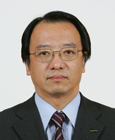
Dr. Jack Sun

VP of R&D and CTO,
TSMC
Abstract
Although the future is difficult to predict, we can foresee semiconductor innovation taking us into ubiquitous computing for smart living and a better world in the 2020s. Energy-efficient Si-wafer based 3D-by-3D (3Dx3D) system scaling with 3D Moore's Law and 3D heterogeneous integration working hand-in-hand may open up many new frontiers of applications and intelligent computing. Transistor count may exceed 50 billion per chip as we move into sub-5 nanometer technology nodes and nanometer manufacturing era. In addition to better 3D low-voltage transistors, breakthroughs in materials and system design are needed to mitigate the rapidly increasing parasitic resistance and capacitance due to dimension scaling. There are many challenges and opportunities for manufacturing science and equipment technology ahead. We need new paradigms in sub-5nm technologies, e.g., from micron to nanometer and angstrom control, from part-per-billion to part-per-trillion defect level, from subtractive to more additive or self-assembly processes, from feedback to feed-forward, and from chip to modular system-level EDA/CAD, design, testing, and reliability assurance, and so on. We are also taking many green fab initiatives and leveraging intelligent IoT for cost-effective and sustainable nanometer manufacturing.
CV
Dr. Jack Yuan-Chen Sun received BSEE degree from National Taiwan University and MS and Ph.D. from the University of Illinois.
He held research and management positions at IBM T.J. Watson Research Center between 1983 and 1997.
He joined TSMC R&D in 1997 as Director of Advanced Module Technology, and then Senior Director of Logic Technology.
He became Vice President of R&D in 2006, and Chief Technology Officer at TSMC in 2009.
He made key contributions to the successful energy efficient CMOS logic SOC platforms with highest routed gate density and computation throughput for the foundry/fabless industry at TSMC.
He advocated a holistic energy efficient 3Dx3D system scaling concept. Throughout his career, he and his co-workers pioneered and set many world records in CMOS, bipolar, and BiCMOS.
Dr. Sun received a number of technical and management awards from IBM, TSMC, professional societies, and government. He was awarded a TSMC Medal of Honor in 2011.
He is an IEEE Fellow for his contributions to CMOS technology.
He received the IEEE EDS J.J. Ebers Award recognition in 2015.
He has authored and co-authored over 200 papers and conference presentations, 12 US patents, and several ROC patents.
"New Era of Electrification and Vehicle Intelligence"
Dr. Haruyoshi Kumura

Fellow,
Nissan Motor Co., Ltd.
Abstract
As the global demand for personal mobility grows continuously, the automotive industry needs to accelerate the development of solutions for the social problems such as environment, energy, resources, traffic accidents and urban congestions. The vehicle electrification and intelligence are key technologies to resolve these social problems. Autonomous drive system technology installed in the latest vehicle will be shared. The examples of recent development for future autonomous drive system will be also shared. Technical issues and challenges for semiconductor will be discussed.
CV
Dr. Haruyoshi Kumura was appointed Fellow in charge of Technology Intelligence of Nissan Motor Co., Ltd. in April 2009.
He graduated from Tokyo Institute of Technology, Master's course of Mechanical Engineering in March of 1981 and joined Nissan Motor.
After assuming several management positions in Nissan's Powertrain and Environment Research Laboratory, he became General Manager in the laboratory in 2003.
His appointment to Vice President in charge of Nissan Research Center in 2005 was quickly followed by his promotion to Corporate Vice President in 2006.
He holds a doctor's degree in mechanical engineering from Yokohama National University.


