Tutorial Speakers
December 13th
Changing semiconductor production management system
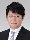
Tetsuya Kubo

Group Manager, Analysis & Data Management Promotion Group, It & Business Transformation Division, Toshiba Corporation Storage & Electronic Devices Solutions Company
Biography
Tetsuya Kubo joined Manufacturing Engineering Research Center of Toshiba Corporation, Yokohama, Japan in 1990. He has been engaged in the research and development of digital control system for semiconductor packaging and automatic machines. Especially he conducted for the development and commercialization of full automatic machine such as flip chip bonding.
Since 2004, he participated in development project of automated systems for 300 mm wafer clean room. In 2006, he has developed the automated construction system (Real Time Dispatcher), and the systems were deployed in Oita and Yokkaichi fab. After that, he promoted the 300mm fab production efficiency that is the world's largest NAND Flash memory production fab in Yokkaichi.
In 2011, he moved to Head Office in Tokyo, and improved the system of design, sales and procurement, and promoted the visualization of management and the use of statistical analysis. His recent interests are promoting Big Data utilization and applying Machine learning to various fields.
Abstract
Due to ongoing cost reduction by refinement and expansion of production scale, NAND Flash memory leads low cost and the market has been growing. The automation system in fab has supported the expansion of this production. The system controls thousands of advanced semiconductor capital tools and controls tens of wafer lots. I explain basic and the development process about the automation system. In recent years, efforts of the Big Data and Machine learning have started, I introduce these Daily changes.
Semiconductors and their band diagrams
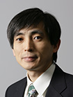
Shinichi Takagi

Professor, School of Engineering, The University of Tokyo
Biography
Shinichi Takagi has received the B.S., M.S. and Ph.D. degrees in electronic engineering from the University of Tokyo, Tokyo, Japan, in 1982, 1984 and 1987, respectively. He joined the Toshiba Research and Development Center, Kawasaki, Japan, in 1987, where he has been engaged in the research on the device physics of Si MOSFETs. From 1993 to 1995, he was a Visiting Scholar at Stanford University, Stanford, CA, where he studied the Si/SiGe hetero-structure devices. Since 2001, he has been working for MIRAI Project, as the leader of New Transistor Structures and Measurement/Analysis Technology Group. In October 2003, he moved to the University of Tokyo, where he is currently working as a professor in the department of Electrical Engineering and Information Systems, School of Engineering. His recent interests are science and technologies of advance MOS devices
Abstract
The recent semiconductor technologies have come to examine a variety of semiconductor materials for practical device use. Also, sizes of those materials often need to be as small as a few nm orders. Here, the band diagram of a semiconductor material is a basis of understanding the physical properties of the semiconductor. This short course will provide the fundamental understanding of the physical origin of the band diagram of typical semiconductor material and the relationship with a variety of physical properties such as the bandgap and the effective mass. Basic physics for undergraduate seniors and first year graduate students majoring in faculty of engineering will be employed for introducing the band diagram. In addition, this presentation will touch on the effects of quantum confinement on the band structures, which is quite important for better understanding of the physical properties of nano-meter-size materials.


