Keynote Speakers
December 15th, 2020
"NVIDIA AI EVOLUTION"
Masataka Osaki

Japan Country Manager, VP Corporate Sales, NVIDIA
Abstract
CV
Masataka (Masa) joined NVIDIA in 2014. As Japan Country Manager, he is responsible for establishing relationships with customers and supporting the eco-system, to expand business in Japan.
Before joining NVIDIA, Masa spent more than 20 years at Texas Instruments Japan, with management roles in many areas such as sales, marketing, technical support, and business development.
Masa has an MBA from Tokyo Metropolitan University.
"New Smart-Microsystems Age Enabled by Heterogeneous Integration of Silicon-Centric and AI Technologies - My Personal View"
Dr.Nicky Lu

Chairman & CEO, Etron Technology
Abstract
After 60 years of development efforts since the 1960s to the current Giga-/Tera-Scale-Integration or System-on-a-Chip era [1], it is expected that Monolithic Silicon IC products using 2-nm CMOS devices will appear soon. The subsequent challenge is whether more novel device structures using heterogeneous materials and 3D-structures will be invented to realize manufacturable 1-nm ICs. On the other hand, through 20 years of efforts since 1999, many Heterogeneous Integration (HI) [2] products, each of which is composed of silicon and non-silicon materials/dice/chiplets, diversified devices/circuits, innovative architectures and multi-dimensional arrangements of dice and other components inside either one Chip-package or on one Module, have been increasingly emerging, especially recently benefiting from a strong driving force stimulated by the IEEE HI Roadmap unveiled in 2018 [2].
This paper presents an exciting, powerful and new Trend of Semiconductors, Intelligent Grand Integration (IGI), which is optimally utilizing Mixed Integration of Monolithic and HI Technologies (Si-4.0 [2]) with embedded 3A’s (Algorithm, Architecture and AI) Design-Intelligences. A key target of IGI technologies is to drive much higher energy efficiency of managing electronic information for more-effective/intelligent future systems with better performance, lower power, higher reliability and smaller form-factor than those of our current systems. One effective way as proposed is to network multiple Self-Smart Microsystems (S-SmS) each of which is designed with 3A’s to a complete system level which can handle huge data processing smartly in its own compact multi-dimensional form factor like in a versatile solid-state micro-universe which has abundant self-contained intelligent functions with maximized speed-power efficiency due to close proximity of electronic/photonic/micro-mechanical operations. It is projected that in such a S-SmS each Joule (energy unit) be able to operate more than 10^20 devices per die allowed by thermodynamics (on the other hand, its performance can reach over hundreds of thousands of TOPS - Tera Operations Per Second) inside and/or across these Microsystems to complete the final system need. Then how powerful a future system can be by networking enough S-SmS units and furthermore how many unprecedented and unexpected applications will be unleashed! To use AI computing systems as an example, it is expected that S-SmS be quickly applied to AI’s edge, device or wearable applications. Moreover, just like the experiences of migrating a Mainframe computer to networked PC Servers, Data servers used in AI Clouds may use such a networked S-SmS architecture to build large systems in order to optimize the energy efficiency and heat dissipation. The trend equally adds values to system’s transition and optimization in Autonomous Car areas, Industrial 4.0 Factory areas, Telecommunication and Computing areas, etc..
Further updates on recent progresses in HI technology development will be presented. More presentations will reveal that the aforementioned both enhanced system-capabilities and energy-efficiency created by prevailing Smart Microsystems of using IC/HI/IGI technologies are accelerating the growth of many intelligence-driven fields such as AI, Cell/Gene Intelligence, Aging/Environment Intelligences, Data Security/Privacy and Space & Earth Interaction Intelligence, etc.. These Pervasive Intelligences (PI) technologies have been widely applied to recently exponentially growing Intelligence^N Applications, which is believed surely to stimulate another exponential SmS-Economy boom enabled by IGI succeeding semiconductor’s world-changing Moore’s Law Economy.
[1] Moore, Electronics, 1965, ISSCC 2003; Dennard, JSSC 1974; Meindl, ISSCC 1993, JSSC 2000.
[2] Lu, ISSCC 2004, FSA 2005, A-SSCC 2016; Chen & Bottoms, IEEE HI Roadmap 2018~now.
CV
As a researcher, design architect, entrepreneur and chief executive, Dr. Lu has dedicated his career to the worldwide IC design and semiconductor industry. He is Chairman, CEO and Founder of Etron Technology, Inc. and co-founded several other high-tech companies including Ardentec and Global Unichip Corp.
Dr. Lu worked for the IBM Research Division and then the Headquarters from 1982 to 1990 and won numerous IBM recognition awards, including an IBM Corporate Award. He co-invented and pioneered a 3D-DRAM technology, known as the Substrate-Plate Trench-Capacitor (SPT) cell, along with its associated array architecture, which has been widely used by IBM and its licensees from 4Mb to 1Gb DRAMs and embedded DRAMs. Dr. Lu designed a High Speed CMOS DRAM (HSDRAM) chip in 1984, 3X faster than normal DRAMs, the concept of which becomes core technologies of many major DRAMs. He was elected as an AdCom member of the IEEE Solid-State Circuits Society from 1977 to 1999, and is on the TPC (Technical Program Committees) of the IEEE International Solid States Circuits Conference (ISSCC) from 1988 to 2002 and of the Symposium on VLSI circuits since 1990, and as Chairman of A-SSCC (2014) and the TPC (2007). He is an IEEE Fellow, the recipient of the IEEE 1998 Solid-States Circuits Award, and a member of National Academy of Engineering of USA.
As a co-architect leading the 8-inch wafer and DRAM/SRAM/LOGIC technology developments for Taiwan’s semiconductor industry in early 1990s, which later creates many Taiwan companies as prominent silicon chip suppliers, Dr. Lu was thus awarded the National Medal of Excellence in Science and Technology, Taiwan, R.O.C. Since 1999 he has pioneered DRAM Known-Good-Die Memory products enabling customers’ 3D stacked-die system chips. This work summoned the new rise of an IC Heterogeneous Integration Era as described in his plenary talk at the 2004 ISSCC, demonstrating a new 3D IC trend in parallel to the Moore’s Law.
Dr. Lu received his B.S. in Electrical Engineering from National Taiwan University and M.S. and Ph.D. in EE from Stanford University. He holds over 24 U.S. patents and has published more than 50 technical papers. He serves as Chairman of TSIA (Taiwan Semiconductor Industry Association) and WSC (World Semiconductor Council), and was Chairman of Global Semiconductor Alliance (GSA, the former FSA) from 2009 to 2011. He is an Outstanding Alumnus of National Taiwan University and a Chair Professor (2005-2007) and an Outstanding Alumnus of National Chiao Tung University.
December 16th, 2020
"Novel sensors from CREST project and open innovation platform, Leafony, connecting sensors to IoT/AI applications" (tentative)
Prof. Takayasu Sakurai
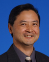
Professor Emeritus, The University of Tokyo
Abstract
Novel sensors based on semiconductor device technologies are described, which are the outcome of the CREST projects on nano-electronics. CREST is a research program funded by the Japanese government. Applications of the sensors are emphasized to show the value of the technologies. In the IoT/AI era, bridging the technologies to applications and services are getting more and more important. An open innovation platform called Leafony is introduced to achieve this goal. By using a newly-developed connection mechanism, Leafony offers electronics modules with a nickel-coin sized footprint, a battery operation and an easy-to-use feature. The platform will accelerate digital transformation by drastically improving the efficiency in the development of IoT and edge-AI systems.
CV
Takayasu Sakurai (IEEE S'77-M'78-SM'01-F'03) received the Ph.D. degree in EE from the University of Tokyo in 1981. In 1981 he joined Toshiba Corporation, where he designed CMOS DRAM, SRAM, RISC processors, DSPs, and SoC Solutions. He has worked extensively on interconnect delay and capacitance modeling known as Sakurai model and alpha power-law MOS model. From 1988 through 1990, he was a visiting researcher at the University of California Berkeley, where he conducted research in the field of VLSI CAD. From 1996, he has been a professor at the University of Tokyo, working on low-power high-speed VLSI, memory design, interconnects, ubiquitous electronics, organic IC's and large-area electronics. He has published more than 600 technical publications including 100 invited presentations and several books and filed more than 200 patents. He is the executive committee chair for VLSI Symposia and a steering committee chair for the IEEE A-SSCC. He served as a conference chair for the Symp. on VLSI Circuits, and ICICDT, a vice chair for ASPDAC, a TPC chair for the A-SSCC, and VLSI symp., an executive committee member for ISLPED and a program committee member for ISSCC, CICC, A-SSCC, DAC, ESSCIRC, ICCAD, ISLPED, and other international conferences. He is a recipient of 2010 IEEE Donald O. Pederson Award in Solid-State Circuits, 2009 and 2010 IEEE Paul Rappaport award, 2010 IEICE Electronics Society award, 2009 IEICE achievement award, 2005 IEEE ICICDT award, 2004 IEEE Takuo Sugano award and 2005 P&I patent of the year award and four product awards. He delivered keynote speech at more than 50 conferences including ISSCC, ESSCIRC and ISLPED. He was an elected AdCom member for the IEEE Solid-State Circuits Society and an IEEE CAS and SSCS distinguished lecturer. He is also a domain research supervisor for nano-electronics area in Japan Science and Technology Agency. He is an IEICE Fellow and IEEE Fellow.
"Rapid Yield Improvement Using Intelligent Data Mining"
Dr. Vivek Jain

Senior Vice President, Technology and Manufacturing Group
Maxim Integrated
Abstract
Entitlement yield is the goal all manufacturing leaders strive to achieve; implementing improvement to get to entitlement yield quickly is critical for capturing the market before competitors, maximizing lifetime product revenue, driving low cost, and meeting customer quality requirements.
However, it is challenging to get to entitlement yield fast given the obstacles:
1. Multiple-month cycle time from start of wafer to getting yield information
2. Multiple yield issues (typical >3) to fix at any given time
3. Multiple iterations to fix a yield issue
4. Initial data looks promising, but high-volume data shows issues – multi factor issue
To be successful, it is important to use a methodology that provides a high-confidence/low-risk path to drive rapid yield improvement. Intelligent data mining is a versatile method that is applicable to new and ramping technologies, and it also addresses excursions in high-volume manufacturing. This method helps leaders understand sources of variation using existing information so that they can quickly figure out the key knobs to drive yield improvement and achieve entitlement yield.
In this paper, we will compare conventional yield improvement methodologies with intelligent data mining. These time-tested methodologies have been validated on deep sub-micron logic and memory as well as state-of-the-art analog and mixed-signal technologies.
CV
Vivek Jain is senior vice president of the Technology and Manufacturing Group for Maxim Integrated, Inc. The Technology and Manufacturing Group includes process development and all manufacturing operations.
Vivek joined Maxim in April 2007 as Vice President of Fab Operations and became Senior Vice President of Manufacturing Operations in 2009. Prior to joining Maxim, Vivek was a Plant Manager at Intel's Technology Development and Manufacturing facility in Santa Clara, CA. At Intel, he oversaw the process technology development and high-volume manufacturing of deep sub-micron logic and Flash memory technologies. Vivek has published more than 30 papers on process technology, semiconductor device reliability and performance. He holds over 10 patents in the field of semiconductor technology.
Vivek holds a BS degree in Chemical Engineering from the Indian Institute of Technology at New Delhi, an MS degree in Chemical Engineering from Penn State University, and an MS degree in Electrical Engineering from Stanford University. He is also a 2014 graduate of the Stanford Graduate School of Business Executive Program.
"Current status and prospective of all-solid-lithium ion batteries" Dr. Takeshi Abe
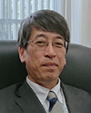
Professor, Department of Energy of Hydrocarbon Chemistry at Graduate School of Engineering, Kyoto University
Abstract
Lithium-ion batteries (LIBs) have been used for almost 30 years.
Lithium-ion batteries have been mainly used for portable electronic devices, and then LIBs have been used for electric vehicles for these 10 years. For the further enhancement of LIBs, increase of energy densities, cycle lives, and safety are required. For the safety issue, all-solid-lithium-ion batteries have attracted much attention. In this conference, I will talk about the advancement of liquid-type lithium-ion batteries at first, and then the current status and prospective of all-solid-lithium-ion batteries will be delivered.
CV
Dr. Abe received his BChE degree from Department of Industrial Chemistry, Faculty of Engineering, Kyoto University in 1992, and he has MS and PhD degrees from Graduate School of Engineering, Kyoto University. Upon completion of his PhD degree in 1996, he joined Graduate School of Engineering, Kyoto University as a Research Associate in 1997 and was promoted to Associate in 2002 and then to Professor in 2009.
Dr. Abe initially devoted to the graphite intercalation compounds and graphite negative electrode for lithium-ion batteries. His current research is various rechargeable batteries,focusing on interfacial phenomena. He has to his credit about peer-reviewed 300 papers and several co-edited books about new technology for advance rechargeable batteries and electrochemistry.
"The outlook of semiconductor industry market in New Normal Age and the impact of US-China on semiconductor supply chain"
Akira Minamikawa

Senior Consulting Director, Semiconductor Value Chain; Technology Fellow, Omdia
Abstract
CV
Akira Minamikawa
Senior Consulting Director
OMDIA (Informa Intelligence LCC)
August 2019 Informa marge IHS Technology group, named OMDIA
Jul,2016 IHS marge Markit
Novemebr, 2010 Acquired by IHS corporation.
December,2006 Acquired by iSuppli corporation.
July, 2004 Established Data Garage Inc.
2003/Apr-04/Feb CLSA Securities, brokerage firm research department technology head & senior analyst
2000/Jun-03/Apr WestLB Securites, brokerage firm research department Director & senior analyst
1996/Jan-00/May IDC Japan, Director of semiconductor research
1990/May-95/Dec Gartner Japan Dataquest semiconductor department, senior analyst
1982/Apr-90/May Motorola /HongKong Motorola Marketing specialist
1982/3 Graduate from Musashi Institute of Technology, electrical engineering department
Main analyst for JEITA world electronics and semiconductor forecast committee from 1997.
Regular speaker of JEITA, SEMI, Semiconductor Industry News and Nikkei Electronics in Japan and Taiwan.
A member of technical examination committee, automotive semiconductor of the Japan Patent Office.
A member of evaluation committee of FeRAM in NEDO.
Regular writer of E-journal, Nikkei Microdevices, Semiconductor industry newspaper.
"SiC and GaN devices for improved power efficiency in automotive and industrial applications"
Dr. Salvatore Coffa

Group VP, R&D General Manager, Power & Discrete, Automotive and Discrete Group, STMicroelectronics
Abstract
The presentation will cover the following points:
The power device evolution and the revolution of compound semiconductors
SiC Power Devices
- Features, applications and roadmaps
- Effects of defects on yield, performances and reliability
GaN Power devices
- Features, applications and roadmaps
- GaN, Smart GaN and heterogeneous integration of GaN and Si
CV
Born in Carlentini (Italy) on September 24th, 1962
1985 - Degree in Physics from University of Catania
1986-1988 fellowship for research activity at STMicroelectronics in Catania
1991 - Ph.D. in Physics from University of Catania
1990-1992 Resident visitor at AT&T Bell Laboratories, New Jersey, USA
March 1993 – September 1994 consultant for CORIMME, a consortium between STMicroelectronics and University of Catania
October 1994-April 2001 Group leader within CNR-IMETEM, a laboratory of the Italian National Council of Research in Catania
May 2001- August 2002 Group manager in STMicroelectronics (on leave on absence from CNR)
From September 2002 Director of Research, Si Optoelectronics and Post-Si Technologies Group, Corporate R&D, STMicroelectronics
From January 2006: Group VP, R&D General Manager, Industrial, Power and Discrete Group, STMicroelectronics
From February 2016: Group VP, R&D General Manager, Power&Discrete, Automotive and Discrete Group, STMicroelectronics
S. Coffa is an ST Company Fellow since 2010
Main achievements
During more than 30 years of research activity Salvatore Coffa has achieved several important results in various fields and, more specifically, a large expertise in the field of technology transfer from basic research ideas to prototypes and then to products and applications. This expertise has been build up combining advanced research work (within or in cooperation with university, research labs, small/medium enterprises) and application to technologies and products within STMicroelectronics.
The main achievements of Salvatore Coffa can be summarised as follows:
- He has developed innovative experiments for exploring the mechanisms of formation and annealing of ion implantation defects in crystalline and amorphous Si. These experiments provide precious inputs for understanding, controlling and simulating defect annealing in modern Si integrated circuits.
- From a detailed understanding of the diffusion mechanisms and electrical properties of Au and Pt in Si, he was able to develop an innovative method for lifetime control (based on ion implantation and diffusion of Au and Pt) which has been then used by STMicroelectronics as lifetime control method in several power devices.
- He has pioneered the work on Si-based optoelectronics. Particularly he has demonstrated that efficient Si-based light sources can be achieved by proper engineering of Si optical properties using Si nanostructures and rare-earths doping. This approach has lead to the fabrication of several innovative Si-based optoelectronics devices (detectors, integrated waveguides, modulators, integrated optical data transmission systems, etc.)
- He has innovated front-end and back-end technologies in the field of power devices introducing new Si power structures (using thrench, thin wafers, etc.) and power structures in semiconductors like SiC and GaN. SiC Power devices are now in full mass production within STMicroelectronics.
- He has authored more than 250 publications on international refereed journals and holds more than 50 patents.


